
Atomic Force Microscope
Room 105a NPIC
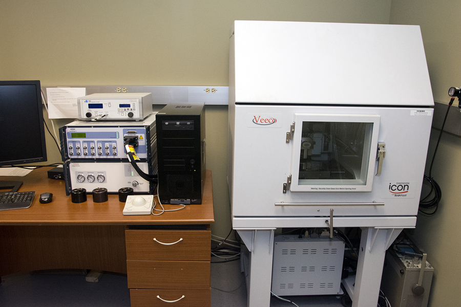
Bruker Dimension Icon AFM
Background
Atomic Force Microscopy (AFM) is a technique for imaging surfaces at the atomic level using a physical probe that scans the sample. The resolution which is achieved is a fraction of a nanometer and is thousand times bigger that the optical microscope resolution. AFM uses a fine, nanometer size tip to map surface morphology and various surface properties through the measured interaction between the tip and the surface. Almost any material can be imaged with minimal or no sample preparation. AFM is very effective in measuring the properties and topography of soft surfaces, especially polymers and biomaterials which are not always easily imaged at high resolution with electron microscopy due to electrostatic charging. Imaging in water/aqueous solution is possible and widely used for biological samples.
The major advantage of atomic force microscopy compared to optical microscopy and electron microscopy is that AFM does not use lenses or beam irradiation. Therefore, it does not suffer from limitations in spatial resolution due to diffraction and aberration, and does not need high vacuum as in electron microscopy or special sample preparations (e.g. staining) as in optical microscopy. Unlike the electron microscope, which provides a two-dimensional projection or a two-dimensional image of a sample, the AFM provides a three-dimensional surface profile in which the height of the surface features can be accurately measured. In addition, samples viewed by AFM do not require metal/carbon coatings that would irreversibly change or damage them.
An AFM uses a cantilever with a very sharp tip to scan over the sample surface. When the tip approaches the surface, an attractive force between the surface and the tip causes the cantilever to deflect towards the surface. However, when the cantilever gets much closer to the surface and almost makes contact with it, a repulsive force appears and causes the cantilever to deflect away from the surface. A laser beam is used to detect cantilever tip deflections towards or away from the surface. By pointing this incident beam onto the backside of the cantilever and monitoring its reflection with a position-sensitive photo detector the cantilever deflections are transformed in direction changes of the reflected beam. A feedback electronic signal is generated to move the cantilever in such way as to keep the reflected laser beam in the center of the photo detector (set point). The value of the feedback signal at each scanned point of the surface of the sample is used to build the 3D image of the surface.
The AFM can be operated in a number of modes, depending on the application. In general, imaging modes are divided into static (contact) modes and dynamic (non-contact or "tapping") modes where the cantilever is vibrated or oscillated at a given frequency. Tapping mode AFM imaging is the preferred technique for most materials.
Applications
Topographic, tribological, roughness, and adhesion characterization of a wide variety of materials; Surface topography imaging of any material in the height range up to 10 um; Phase imaging to generate materials contrast in polymer composites and blends, protein adsorption, self –assembled monolayers; Polymers, polymer coatings and thin films, nanomaterials, graphene, carbon nanotubes, metal-oxide and metal nanowires; Characterization of nanoparticles from different materials: metal, metal/organic, synthetic polymer, biopolymer, nanorods, quantum dots etc; High tech applications: digital data storage, flat displays, optics, MEMS devices; Commercial product testing – nano- and micro-sized ingredients in sport goods, automotive tires, hair treatment products; Imaging the fine structure of metals and adsorbed species on metals and semiconductors; Studies of friction and wear; Nanoscale surface roughness measurements of high‐performance materials; Stiffness or hardness measurement and imaging of polymer films and biomaterials; Bacterial cell imaging and mechanical testing, lipid membranes imaging
Specifications
- AFM modes: ScanAsyst, PeakForce Tapping, TappingMode (air), Contact Mode, Lateral Force Microscopy, Phase Imaging, Lift Mode, MFM, Force Spectroscopy, Force Volume, Surface Potential, Force Spectroscopy; PeakForce QNM, PeakForce TUNA
- X-Y scan range: 90μm x 90μm typical, 85μm minimum
- Z range: 10μm typical in imaging and force curve modes, 9.5μm minimum
- Vertical noise floor: <30pm RMS in appropriate environment typical imaging bandwidth (up to 625Hz)
- X-Y position noise (closed-loop): <0.15 nm RMS typical imaging bandwidth (up to 625Hz)
- X-Y position noise (open-loop): <0.10 nm RMS typical imaging bandwidth (up to 625Hz)
- Z sensor noise level (closed-loop): 35pm RMS typical imaging bandwidth (up to 625Hz); 50pm RMS, force curve bandwidth (0.1Hz to 5kHz)
- Integral nonlinearity (X-Y-Z): <0.5% typical
- Sample size/holder 210 mm vacuum chuck for samples, 210 mm diameter, 15 mm thick
- Motorized position stage (X-Y axis): 180mm × 150mm inspectable area; 2μm repeatability, unidirectional; 3μm repeatability, bidirectional
- Microscope optics: 5-megapixel digital camera; 180 μm to 1465 μm viewing area; Digital zoom and motorized focus
- Controller: NanoScope V
- Workstation: Integrates all controllers and provides ergonomic design with immediate physical and visual access
- Vibration isolation: Integrated, pneumatic
- Acoustic isolation: Operational in environments with up to 85 dBC continuous acoustic noise