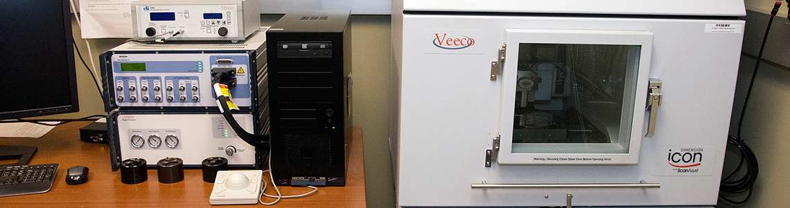
Three-dimensional surface topographic imaging. Nano-scale mapping of mechanical properties (elastic modulus, surface adhesion and dissipation), electrical properties (conductivity, capacitance, piezoelectric response), magnetic properties, and heat trasfer properties (thermal conductivity, temperature distribtion) are possible
Applications: imaging of thin films and coatings, nanostructures, batteries and energy storage, biocompatibility, corrosion and antifouling, data storage, optics, photovoltaics, semiconductor and microelectronic devices, sensors and actuators, tribology (hardness, lubrication, and wear). Imaging the structure of biological molecules, cellular components, cells or tissues